Researchers from North Carolina State University (NC State) have published their findings in a new paper demonstrating a method for printing flexible circuits onto curved surfaces.
Such surfaces include a latex glove and a contact lens. How did they do this? Read on for the answers.
Printing Curved Circuits
Directly printing circuits, in both 2D and 3D is nothing new, but each process comes with its own set of challenges, and as yet, it has been tricky to print high-resolution, complex patterns of metal nanowires on curvilinear substrates.
The team from NC State has successfully developed a new method that does exactly that, and the process has been named as MIMIC, which stands for “MIcroMolding In Capillary”.
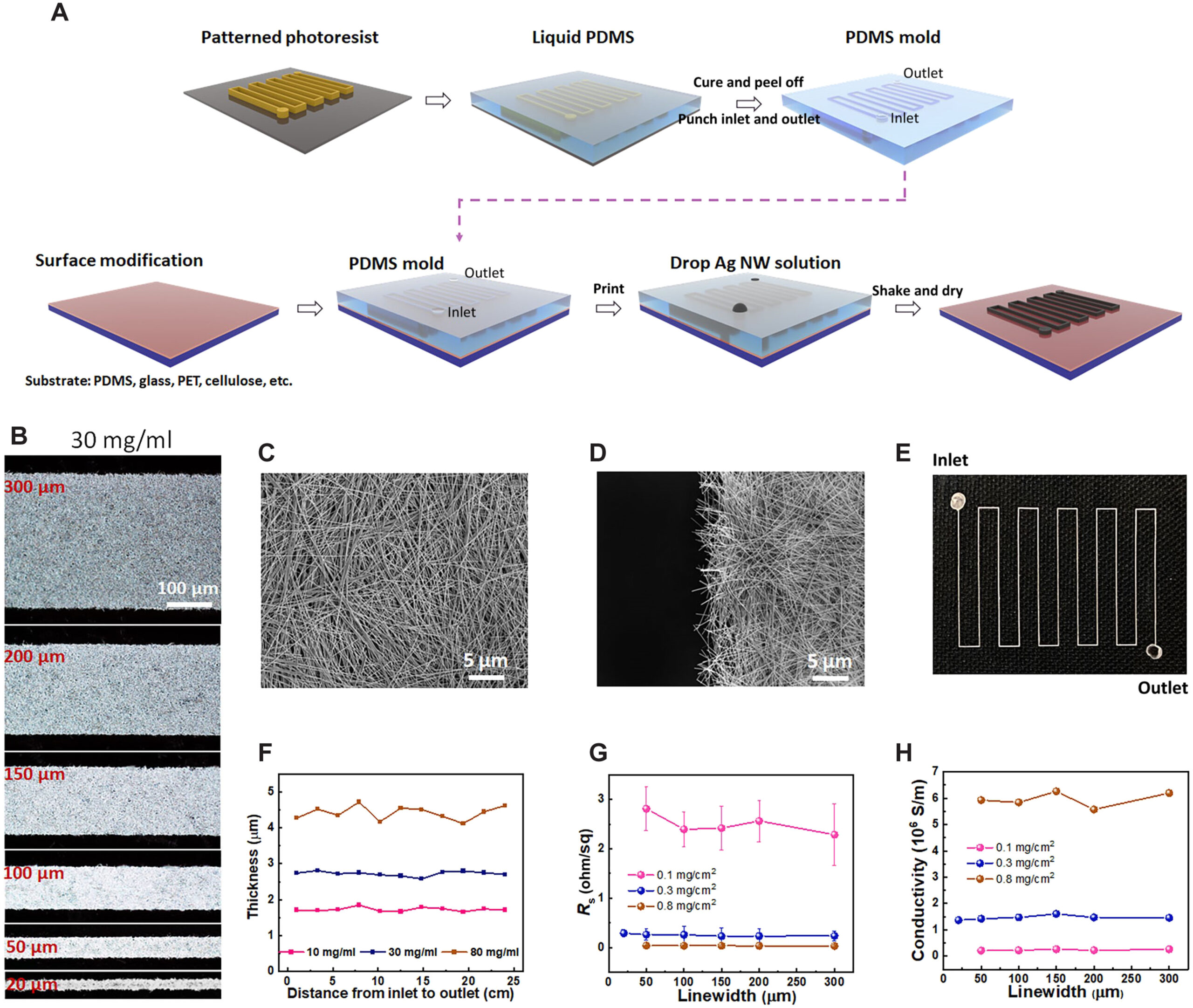
The process works by first using a (UV) photolithography step to pattern a template in a photoresist material featuring a set of microscale grooves representing the circuit to be printed.
Next, a liquid silicone (PDMS) is poured onto the photoresist, and cured, before being peeled off to leave a microchannel in the shape of the photoresist in the cured silicone. Inlet and outlet holes are punched into the PDMS mold.
The mold is placed onto the curved (or flat) substrate on which the circuit is required, and a silver nanowire and ethanol solution (the ink) is dropped into the inlet.
Capillary action then pulls the solution through the microchannels where the mold is shaken and the ink is left to dry at room temperature.
After removing the mold, the desired circuit track geometry is left intact on the surface.
You can see the process in the image below.

“There are many existing techniques for creating printed electronics using various materials, but limitations exist,” says Yong Zhu, Professor of Mechanical and Aerospace Engineering at NC State and corresponding author on the paper.
“One challenge is that existing techniques require the use of polymer binding agents in the ‘ink’ you use to print the circuits. This impairs the circuit’s conductivity, so you have to incorporate an additional step to remove those binding agents after printing. A second challenge is that these printing techniques typically require you to print on flat surfaces, but many applications require surfaces that aren’t flat.”
Uniform Thickness
The researchers performed various tests on the deposited circuits and found that the sheet resistances and conductivities appear to be uniform along the pattern. This was due to the ink reaching equilibrium after the microchannel was completely filled.
“We’ve developed a technique that doesn’t require binding agents and that allows us to print on a variety of curvilinear surfaces,” says Yuxuan Liu, PhD student and first author of the paper.
“It also allows us to print the circuits as grid structures with uniform thickness.”
The researchers printed the nanowires on a variety of substrates including glass, polyethylene terephthalate (PET), PDMS, cellulose film, a latex glove, and a plastic petri dish.
Three functional prototypes were also manufactured to demonstrate the process.
These were a “smart” contact lens with built-in circuits for measuring the fluid pressure of the eye, a flexible, transparent electrode with circuits printed in a grid pattern, and a latex glovewith circuits serving as pressure sensors.
“We think this could be scaled up pretty easily, in terms of manufacturing,” said Zhu.
“We’re open to talking with industries who are interested in exploring this technique’s potential.”
And we know what you’re thinking…
Is this really 3D printing?
And our answer to that question is…
The ink was printed on a curved surface, in three dimensions.
So from our perspective, it is certainly a form of 3D printing, even if it’s not exactly additive manufacturing in the usual form that we write about on these pages.
Take a look at the research paper, titled “Curvilinear soft electronics by micromolding of metal nanowires in capillaries” (at this link) and decide for yourselves!


