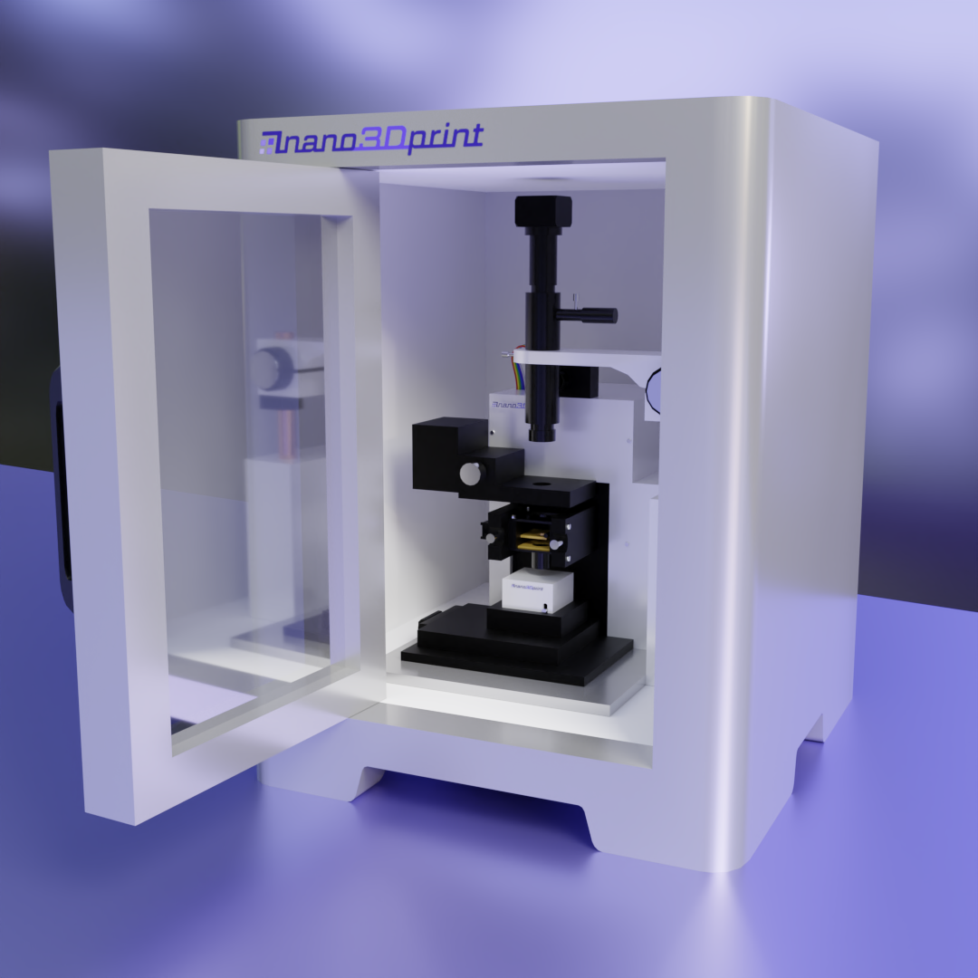
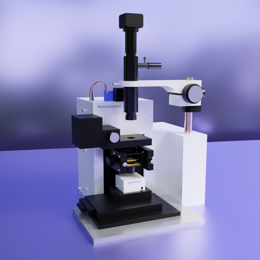
California-based nano3Dprint has launched their groundbreaking D4200S printer, capable of printing with a 20-nanometer resolution, making it the highest resolution of any additive manufacturing system currently available.
You can see a render of the D4200S in the image below.

Yes, nano3Dprint is not just a clever name chosen for marketing purposes, because the D4200S can actually print nanoscale features, making it ideal for both research, and nanoscale (and microscale) fabrication in numerous domains requiring high levels of precision.
Wide Range of Inks
The fundamental technology of the D4200S 3D printer combines the merging of atomic force microscope (AFM) technology with fluid delivering carbon nanotube tips. The printer’s nano-deposition mode is capable of printing with a range of between 20 nanometers to 250 microns, while the high-speed micro-deposition mode can handle feature sizes ranging from 5 microns to 400 microns.
The high-precision, ultra reliable positive displacement micro-deposition mode print head is capable of precisely metering functional inks with viscosities ranging from 1mPa·s to 54000 mPa·s. Such inks include gold, silver, copper, polymers, metallic oxides, dielectrics, organic compounds, photosensitive polymers and more.

This wide range of ink compatibility, combined with fine control over the resolution and precision is perfect for a wide range of applications including flexible electronics, prototypes, maskless lithography, mask repair, bioprinting, tissue engineering, and even the printing of computer chips!
Atomic Force Microscopy
You may be wondering how users can monitor that the prints are going well, when operating at such tiny scales. nano3Dprint has this covered, as the D4200S also includes atomic force microscopy capabilities for analysis.
The atomic force microscope is equipped with a 50 micron XYZ scanner allowing for precise positioning of the AFM probe tip in three dimensions. The AFM works by scanning the probe tip over a sample surface and measuring the forces between the tip and the sample. The XYZ scanner moves the tip in the x, y, and z directions, allowing it to scan the entire surface of the sample and create a three-dimensional map of its topography.
The printer also comes equipped with a video optical microscope, with 400x zoom and 2 μm resolution.

“Our goal with introducing the D4200S is to provide accessible next-generation technology for top-tier research labs and innovative startups alike,” says Gretta Perlmutter, nano3Dprint Product Success Manager.
“For example, one D4200S printer can essentially replace all the equipment necessary for lithographic processing in a cleanroom. While a fully-equipped cleanroom could cost millions of dollars, the D4200S is a fraction of the cost.”
How small a fraction? The D4200S is available for order right now, with a minimum down payment of $62,500. The total cost of the printer is $250,000, with shipments starting later this year. If you’re in the market for a nano-scale resolution printer, then you can head on over to the product webpage for more information at this link.
| D4200S Specifications | |
| Tip Sizes | 200 μm, 50 μm, 25 μm, 10 μm, 5 μm, 1μm, 500 nm, 200 nm, and 20 nm |
| Supported inks | Metal, Metallic Oxides, Polyimide, Ag, Au, Pt, Pd, Dielectrics, OrganicSemiconductors, Photosensitive Polymers, Biomolecules, etc. |
| Sample size | Up to 5 cm x 5 cm x 5 cm |
| PrecisionStage | XYZ < 3 nm, 3 x 6 x 2 cm Travel(Custom sizes available) |
| Modes | Micro Deposition, Nano Deposition, Topographical Analysis |
| Video Optical Microscope | Zoom to 400x, 2 μm resolution |
| Stage and Control Box | Compact Table-Top Design7.5 in x 12 in |
Come and let us know your thoughts on our Facebook, Twitter, and LinkedIn pages, and don’t forget to sign up for our weekly additive manufacturing newsletter to get all the latest stories delivered right to your inbox.


